The competition between Intel and AMD has been heating up in the last few years as Intel has released chips fabbed with their 14nm++ process and AMD has been using TMSC’s 7nm process. In the wake of the two semiconductor titans clashing, a debate between the merits of 14nm++ and 7nm has sprung up with some confusion about what those numbers actually measure. Not taking either number at their face value, [der8auer] decided to extract a transistor from both Intel’s and AMD’s latest offerings to try and shed some light.
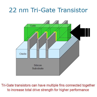
Much of the confusion comes from the switch to the FinFET process. While older planar transistors could be thought of as largely 2d structures, FinFET’s are three dimensional. This means that the whole vertical fin can act as a gate, greatly reducing leakage. It is this fin or gate that [der8auer] is after. On each chip, a thin sliver from the L1 cache was chosen as caches tend to be fairly homogenous sections with transistors that are fairly indicative of the rest of the chip. Starting with a platinum gas intersecting with a focused ion beam on the surface of the chip, [der8auer] built a small deposit of platinum over several hours. This deposit protects the chip when he later cut it at an angle, forming a small lamella 100 micrometers long. In order for the lamella to be properly imaged by the scanning electron microscope, it needed to be even thinner (about 200 to 300nm).
Eventually, [der8auer] was ultimately able to measure the gate height, width, spacing, and other aspects of these two chips. The sheer amount of engineering and analysis that went into this project is remarkable and we love the deep dive into the actual gates that make up the processors we use. If you’re looking for a deep dive into the guts of a processor but perhaps at a more macro scale, why not learn about a forgotten Intel chip from the 1970s?
Thanks [paulvdh] for sending this one in!
Recent Comments